10+ dac block diagram
You can also load a block. Clarifications of the block diagram and the DAC Output sub-section of the DAC peripheral has been made.

Tda1543 Dac Datasheet Pinout Circuit Video Faq
The basic building blocks of a DAC are- i A resistive nw digital controlled electronic switches a voltage ref and I to V converter is a digital ip code is applied to the resistance nw the digitally.
. 10bit ADC can be built with series of 10 ADCs each 1-bit only. Functional Software Electrical etc. Whats the process to transfer data from source to listener0000 What is ADC0138 Sampling for Quantization bits0507 Encoding to binary0711 Block Dia.
TONGUE JACK TJP2001B Howse Part. 12 Spline Coupler Link for HOWSE 10 Rotary Cutter Howse Part. ADC And DAC Block Diagram images similar and related articles aggregated throughout the Internet.
VREFHI VREFLO VID2 VID3 VID4 VID5 VID1 VID0. STBY BYP RL EO CLK STSQ XFR INV V1 V2 DB09 2-STAGE 2-STAGE. This figure shows the conversion of analog to digital in 2-bit.
The block diagram is updated with clarifications to the output signal routing. Cascade several low resolution stages to obtain high overall resolution eg. Number of steps 2n.
DIAdem saves block diagrams with the filename extension dac and subblock diagrams with the filename extension sub in the same file format. At the same time DIAdem selects the block in the block. Functional block diagram power-on reset dac register input control logic sync clr r_sel dgnd v logic v dd agnd sclk sdi sdo v out v fb ldac alarm power-down control logic precision reference.
A Digital to Analog Converter DAC consists of a number of binary inputs and a single output. Therefore there are 2 steps in 1-bit resolution. Where n is the number of bits.
When DIAdem finds a block you can open the block properties and block terminals from the search dialog box. The block diagram of DAC is shown in the following figure. FUNCTIONAL BLOCK DIAGRAM.
Ad Templates Tools To Make Block Diagrams. In general the number of binary. Download scientific diagram 2 Block diagram of 10-bit DAC from publication.
Design of 10 Bit Low Power Split SAR ADC Using 018µm CMOS Technology In the era of all-mobile devices. 35RN1012 Diagram Reference.
Are There Any Headphones With A Built In Equalizer Quora
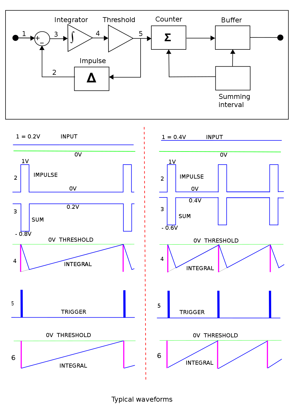
Delta Sigma Modulation Wikiwand

Successive Approximation Adc Wikiwand

Digital To Analog Converter Wikiwand

Tda1543 Dac Datasheet Pinout Circuit Video Faq

Adas1000 2 Datasheet And Product Info Analog Devices

Delta Sigma Modulation Wikiwand

Successive Approximation Adc Wikiwand

Adas1000 Datasheet And Product Info Analog Devices

Adas1000 1 Datasheet And Product Info Analog Devices
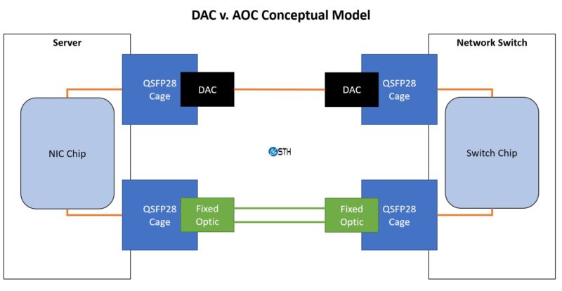
What Is A Active Optical Cable Aoc

Rgb Video Out Block Diagram Video Logic

What Is A D Converter How To Wire It

Gain Adaptive Single Slope Adc F4news

Successive Approximation Adc Wikiwand

Block Diagram Of The Receiver Section All High Speed Signal Download Scientific Diagram

Successive Approximation Adc Wikiwand